C
EK-RA8D1 Kit
This topic provides board-specific information about Renesas' EK-RA8D1.
Board features
- R7FA8D1BHECBD MCU featuring ARM Cortex-M85, 2 MB Flash, 1 MB SRAM
- 4.5” 480x854 LCD Touch Display
- 64 MB SDRAM
- 64MB External Octo-SPI Flash
Supported color depths
The reference port for this board supports 16bpp color depth. See QUL_COLOR_DEPTH and Color depth for more information.
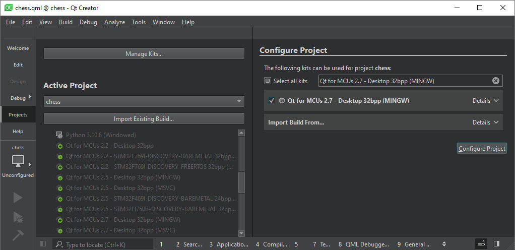
Building applications with prebuilt Qt Quick Ultralite libraries
- Open the CMake project file for the example you want to build.
- In the Configure Project window:
- Select the kit you created earlier. For example, Qt for MCUs 2.10.1 - Desktop 32bpp.
- Select Configure Project.
Once the project is configured, select Run or press Ctrl+r on your keyboard to build and flash the binary to the target.
Reading debug messages
By default, log data is redirected to JLink CDC UART Port (USB COM port).
Port settings
| Setting | Value |
|---|---|
| Bits per second | 115200 |
| Data bits | 8 |
| Parity | None |
| Stop bits | 1 |
| Flow control | None |
Debugging
Renesas e2 studio
Renesas e2 studio lets you debug a project using a custom configuration.
- Create a Bare Metal - Minimal project for EK-RA8D1.
- Build the project.
- Copy the Qt Quick Ultralite .elf file into the Debug folder of the e2 studio project.
- Take a copy of the original .sbd file and rename it with same name as the Qt Quick Ultralite .elf file.
- Select Run from the top menu.
- Select Debug Configurations....
- Select Renesas GDB Hardware Debugging.
- Set the Qt Quick Ultralite .elf to the C/C++ Application:.
- Select Apply and Close.
- Select Launch in 'Debug' mode.
Default FSP Configuration in Renesas e2 studio
Note: Use the default value for the property if not specified in the table.
BSP
| Property | Value |
|---|---|
| RA Common > Main stack size (bytes) | 65536 |
| RA Common > Heap size (bytes) | 262144 |
Clocks
| Clock setting | Value |
|---|---|
| SCICLK Src | PLL1P |
| PLL2 Src | XTAL |
| PLL2 Mul | x40.0 |
| LCDCLK Src | PLL2P |
| OCTASPICLK Src | PLL2P |
Note: SCICLK should be 120MHz
Note: LCDCLK should be 200MHz
Note: OCTASPICLK should be 100MHz
Stacks
Add the following stacks and configure them:
Analog > ADC (r_adc)
| Property | Value |
|---|---|
| Module > General > Name | g_adc0 |
| Module > Input > Channel Scan Mask > Channel 2 | Selected |
| Pins > AN02 | P006 |
Connectivity > I2C Master (r_iic_master)
| Property | Value |
|---|---|
| Module > Name | g_i2c_touch |
| Module > Channel | 1 |
| Module > Rate | Standard |
| Module > Rise Time (ns) | 120 |
| Module > Fall Time (ns) | 120 |
| Module > Duty Cycle (%) | 50 |
| Module > Slave Address | 0x00 |
| Module > Address Mode | 7-bit |
| Module > Timeout Mode | Short Mode |
| Module > Callback | touch_i2c_callback |
| Module > Interrupt Priority Level | Priority 6 |
| Pins > SCL1 | P512 |
| Pins > SDA1 | P511 |
Connectivity > UART (r_sci_b_uart)
| Property | Value |
|---|---|
| Module > General > Name | g_uart0 |
| Module > General > Channel | 9 |
| Module > General > Data Bits | 8bits |
| Module > General > Parity | None |
| Module > General > Stop Bits | 1bit |
| Module > Interrupts > Callback | user_uart_callback |
| Pins > RXD9 | PA15 |
| Pins > TXD9 | PA14 |
Graphics > D/AVE 2D Port Interface (r_drw)
| Property | Value |
|---|---|
| Common > Allow Indirect Mode | Enabled |
| Common > Memory Allocation | Custom |
| Module D/AVE 2D Port Interface (r_drw) > D2 Device Handle Name | d2_handle0 |
| Module D/AVE 2D Port Interface (r_drw) > DRW Interrupt Priority | Priority 2 |
Graphics > Graphics LCD (r_glcdc)
| Property | Value |
|---|---|
| Module > General > Name | g_display0 |
| Module > Interrupts > Callback Function | glcdc_callback |
| Module > Interrupts > Line Detect Interrupt Priority | Priority 12 |
| Module > Input > Graphics Layer 1 > General > Horizontal size | 480 |
| Module > Input > Graphics Layer 1 > General > Vertical size | 854 |
| Module > Input > Graphics Layer 1 > Framebuffer > Number of framebuffers | 2 |
| Module > Input > Graphics Layer 1 > Framebuffer > Section for framebuffer allocation | .sdram |
| Module > Output > Timing > Horizontal total cycles | 559 |
| Module > Output > Timing > Horizontal active video cycles | 480 |
| Module > Output > Timing > Horizontal back porch cycles | 5 |
| Module > Output > Timing > Horizontal sync signal cycles | 2 |
| Module > Output > Timing > Horizontal sync signal polarity | Low active |
| Module > Output > Timing > Vertical total lines | 894 |
| Module > Output > Timing > Vertical active video lines | 954 |
| Module > Output > Timing > Vertical back porch lines | 20 |
| Module > Output > Timing > Vertical sync signal cycles | 3 |
| Module > Output > Timing > Vertical sync signal polarity | Low active |
| Module > Output > Timing > Data Enable Signal Polarity | High active |
| Module > Output > Timing > Sync edge | Falling edge |
| Module > Output > Format > Color format | 24bits RGB888 |
| Module > TCON > Hsync pin select | LCD_TCON1 |
| Module > TCON > Vsync pin select | LCD_TCON0 |
| Module > TCON > Panel clock division ratio | 1/8 |
MIPI Display (r_mipi_dsi)
| Property | Value |
|---|---|
| Module > General > Name | g_display0 |
| Module > Low Power > Ultra Low Power State Wakeup Period | 290 |
MIPI Physical Layer (r_mipi_phy)
| Property | Value |
|---|---|
| Module > DSI PLL Frequency | 560 |
Input > External IRQ (r_icu)
| Property | Value |
|---|---|
| Module > Name | g_touch_irq |
| Module > Channel | 3 |
| Module > Trigger | Falling |
| Module > Digital Filtering | Enabled |
| Module > Digital Filtering Sample Clock | PCLK / 64 |
| Module > Callback | touch_irq_cb |
| Module > Pin Interrupt Priority | Priority 5 |
Note: Ensure that the mode of pin P510 is Output mode (Initial Low). The mode is changed to Input mode during the GT911 initialization process.
Storage > OSPI Flash (r_ospi_b)
| Property | Value |
|---|---|
| Common > Memory-mapping Support > Prefetch Function | Enable |
| Common > Memory-mapping Support > Combination Function | 64 Byte |
| Common > Memory-mapping Support > XiP Support | Disable |
| Common > DMAC Support | Enable |
| Common > Autocalibration Support | Enable |
| Common > DOTF Support | Disable |
| Module > General > Name | g_ospi_b |
| Module > General > Channel | 1 |
| Module > General > Initial Protocol Mode | SPI (1S-1S-1S) |
| Module > General > Initial Address Bytes | 4 |
| Module > General > Write Status Bit | 0 |
| Module > General > Write Enable Bit | 1 |
| Module > General > Sector Erase Size | 4096 |
| Module > General > Block Erase Size | 262144 |
| Module > General > Command Set Table | (empty) |
| Module > General > Command Set Table Length | 0 |
| Module > Defaults > Command Definitions > Page Program Command | 0x12 |
| Module > Defaults > Command Definitions > Read Command | 0x0B |
| Module > Defaults > Command Definitions > Write Enable Command | 0x06 |
| Module > Defaults > Command Definitions > Status Command | 0x05 |
| Module > Defaults > Erase Command Definitions > Sector Erase Command | 0x2121 |
| Module > Defaults > Erase Command Definitions > Block Erase Command | 0xDCDC |
| Module > Defaults > Erase Command Definitions > Chip Erase Command | 0x6060 |
| Module > Defaults > Dummy Cycles > Memory Read Dummy Cycles | 3 |
| Module > Defaults > Dummy Cycles > Status Read Dummy Cycles | 0 |
| Module > High-speed Mode > Auto-Calibration > Data latching delay | 0 |
| Module > High-speed Mode > Auto-Calibration > Auto-Calibration Address | 0x90002000 |
| Module > High-speed Mode > Command Definitions > Page Program Command | 0x1212 |
| Module > High-speed Mode > Command Definitions > Dual Read Command | 0xEEEE |
| Module > High-speed Mode > Command Definitions > Write Enable Command | 0x0606 |
| Module > High-speed Mode > Command Definitions > Status Command | 0x0505 |
| Module > High-speed Mode > Command Definitions > Sector Erase Command | 0x2121 |
| Module > High-speed Mode > Command Definitions > Block Erase Command | 0xDCDC |
| Module > High-speed Mode > Command Definitions > Chip Erase Command | 0x6060 |
| Module > High-speed Mode > Protocol | Dual data rate OPI (8D-8D-8D) |
| Module > High-speed Mode > Command Length Bytes | 2 |
| Module > High-speed Mode > Memory Read Dummy Cycles | 10 |
| Module > High-speed Mode > Status Read Dummy Cycles | 4 |
| Module > Chip Select Timing Setting > Command Interval | 2 |
| Module > Chip Select Timing Setting > Pull-up Timing | No Extension |
| Module > Chip Select Timing Setting > Pull-down Timing | No Extension |
| Pins > OM_CS1 | P104 |
| Pins > OM_DQS | P801 |
| Pins > OM_ECSINT1 | P105 |
| Pins > OM_RESET | P106 |
| Pins > OM_SCLK | P808 |
| Pins > OM_SIO0 | P100 |
| Pins > OM_SIO1 | P803 |
| Pins > OM_SIO2 | P103 |
| Pins > OM_SIO3 | P101 |
| Pins > OM_SIO4 | P102 |
| Pins > OM_SIO5 | P800 |
| Pins > OM_SIO6 | P802 |
| Pins > OM_SIO7 | P804 |
Timers > Timer, General PWM (r_gpt)
| Property | Value |
|---|---|
| Common > Pin Output Support | Enabled |
| Module > General > Name | g_timer_for_ospi_b |
| Module > General > Channel | 0 |
| Module > General > Mode | Periodic |
| Module > General > Period | 0x10000 |
| Module > General > Period Unit | Raw Counts |
| Module > Output > GTIOCA Output Enabled | False |
| Module > Output > GTIOCB Output Enabled | False |
Timers > Timer, General PWM (r_gpt)
| Property | Value |
|---|---|
| Common > Pin Output Support | Enabled |
| Module > General > Name | g_timer_PWM |
| Module > General > Channel | 7 |
| Module > General > Mode | Saw-wave PWM |
| Module > General > Period | 10 |
| Module > General > Period Unit | Milliseconds |
| Module > Output > Duty Cycle Percent | 75 |
| Module > Output > GTIOCB Output Enabled | True |
| Pins > GTIOCB | P404 |
Note: When setting the GTIOCB pin, ensure that the Operation Mode of the GPT Timer is GTIOCA or GTIOCB, and pin P404 is in Peripheral mode.
Known issues or limitations
- The external 64 MB Octo-SPI flash memory is not supported in the technology preview.
Available under certain Qt licenses.
Find out more.
